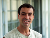
Educational Background
- B.S. 1986, M.S. Physics, 1988. Moscow Institute of Physics and Technology.
- Ph.D., Physics, 1993.
Institute for Physical Problems, Russian Academy of Sciences.
Research Interests
- Surface science
- Scanning probes
- Low temperature physics
Contact Information
Email: [email protected]
Phone: 972-883-6537
Office: BE 2.310
Igor Altfeder
Igor Altfeder received PhD in physics from Institute for Physical Problems of Russian Academy of Sciences. Since 1996 till 2000 he worked in the Rowland Institute for Science ( Cambridge, MA) as a postdoctoral fellow. His specialization is surface science and scanning probe surface microscopy. In 2001 he became a research associate at Harvard University, where he continued experimental study of low-dimensional materials. In 2004 Igor joined NanoTech at UTDallas as research scientist. Here, Igor studies the properties of carbon nanostructures using scanning probes.
Selected Publications
Dual-probe scanning tunneling microscope for study of nanoscale metal-semiconductor interfaces, W. Yi, I. Kaya, I. Altfeder et al., Review of Scientific Instruments, 76, 063711 (2005)
Anisotropic Metal-Insulator Transition in Epitaxial Thin Films, I. B. Altfeder, X. Liang, T. Yamada, D. M. Chen,V. Narayanamurti, Physical Review Letters, 92, 226404 (2004).
Imaging Subsurface Reflection Phase with Quantized Electrons, I. B. Altfeder, V. Narayanamurti, D. M. Chen, Physical Review Letters, 88, 206801 (2002).
Observations of Conduction Band Structure of 4H- and 6H-SiC, I. Shalish, I. B. Altfeder, V. Narayanamurti, Physical Review B, 65, 073104 (2002).
Confinement-Enhanced Electron Transport Across a Metal-Semiconductor Interface, I. B. Altfeder, J. A. Golovchenko, V. Narayanamurti, Physical Review Letters, 87, 056801 (2001).
Bistability in scanning tunneling spectroscopy of Ga-terminated Si(111), I. B. Altfeder, D. M. Chen, Physical Review Letters, 84, 1284 (2000).
Imaging Buried Interfacial Lattices with Quantized Electrons, I. B. Altfeder, D. M. Chen, K. A. Matveev, Physical Review Letters, 80, 4895 (1998).
Electron Fringes on a Quantum Wedge, I. B. Altfeder, K. A. Matveev, D. M. Chen, Physical Review Letters, 78, 2815 (1997).
Hexagonal phase with a mosaic structure of charge density waves observed by STM at the surface of NbSe 3 crystal, I. B. Altfeder, S. V. Zaitsev-Zotov, Physical Review B, 54, 7694 (1996).
Low temperature STM with a reliable piezoelectrical coarse approach mechanism, I. B. Altfeder, A. P. Volodin, , Review of Scientific Instruments, 64, 3157 (1993).
Electrical and magnetic properties of variously annealed Bi(Pb)SrCaCuO thick films, I. Kirschner, S. Leppavuori, R. Laiho, I. Altfeder et al., Z. Phys.B, 85, 175 (1991).
Updated: November 4, 2005
